


Scanning Microwave Impedance Microscopy (sMIM) is a new mode of imaging using an atomic force microscope (AFM). PrimeNano’s ScanWave sMIM modules produce high quality images of local electrical properties with better than 50 nm resolution. The core of our technical approach is to utilize microwave reflections from a nm scale region of the sample directly under the MIM probe. The magnitude and phase of these reflections is dominated by the local electrical properties. The ScanWave sMIM measures these reflections as a function of position to create images of variations in dielectric constant and conductivity.
The ScanWave™ system provides two channels as output to the host AFM that can then be viewed as images in the AFM software. The two channels represent the permittivity (ε) and the conductivity (σ) of the imaged area. If the sample is a doped semiconductor (a non-linear) material, ScanWave™ can provide the dC/dV amplitude (carrier concentration) and phase (carrier type: n or p) as well as the dR/dV amplitude.
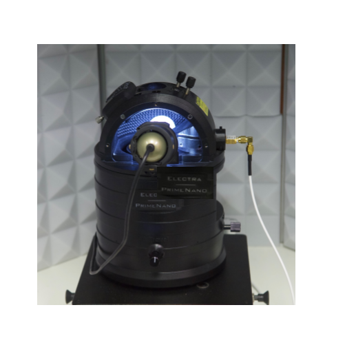
How ScanWave™ Works
ScanWave™ sends microwaves to the probe tip via a fully shielded path.
The microwaves create a near-field electromagnetic wave at the the probe tip that interacts with the sample surface and subsurface.
After the near-field interacts with the sample, a portion of the microwave power is reflected back through the same shielded path to the ScanWave™ electronics for filtering, demodulating, and processing.
As the probe moves across the sample, the reflected microwaves vary in amplitude and phase due to variations in the local electrical properties under the probe tip.
The ScanWave™ software calibrates the reflected signal from the probe-sample interface to create a capacitive and a resistive image that are displayed by the AFM simultaneously with the topography image or images.

Characterization Of Insulated-Gate Bipolar Transistor

Vertical Insulated Gate Bipolar Transistors (IGBTs) are one of the most important types of discrete power transistors. These devices were developed to have more efficient operation and faster switching. The IGBT combines the simple gate-drive characteristics of MOSFETs with the high-current and low-saturation-voltage capability of bipolar transistors.1
CMOS

(http://www.azonano.com/article.aspx?ArticleID=4207)
Spontaneous Domain Walls In Ferroelectric Crystals
Ferroelectric materials possessing spontaneous polarizations have been widely employed in data storage1,2 and nano-scale transistor devices3. In these applications ferroelectric domains are purposefully polarized for device structures to realize certain functions. In recent years, the ferroelectric domain walls (DWs), where the order parameter changes drastically within a narrow width (sub-to-few nanometers) 4-8, have become the subject of intense scientific research9-11. In particular, the unexpected electrical conduction at ferroelectric DWs12-15 is highly attractive because of the possibility to create and control nano-scale 1D/2D conductive paths in wide band gap insulators.
LiTaO3
 (http://www.primenanoinc.com/smim_wp3/?page_id=756)
Conductivity Studies Of Graphene
Graphene has attracted enormous interest and intense research activities due to its rich physical properties in fundamental research and versatile potentiality to revolutionize many applications, especially in electronics and opto-electronics1,2,3. The unique properties of graphene for electrical applications makes it a focal point for next generation microelectronics. Imaging the electrical properties of graphene presents specific challenges to researchers. sMIM reduces the technical difficulties of preparing often small flakes or films on non-conducting substrates for electrical measurement by eliminating the need for a conductive path. sMIM directly probes the grain structures and local variations in conductivity differentiating between conductive, semi conductive, and insulating regions. Below are presented several examples of sMIM measurements on differently prepared graphene.
Moire Patterns on Single Layer Graphene deposited on BN

After surface Measurement

(Seeing through Walls at the Nanoscale: Microwave Microscopy of Enclosed Objects and Processes in Liquids. ACS Nano 10, 3562–3570 (2016).)

