


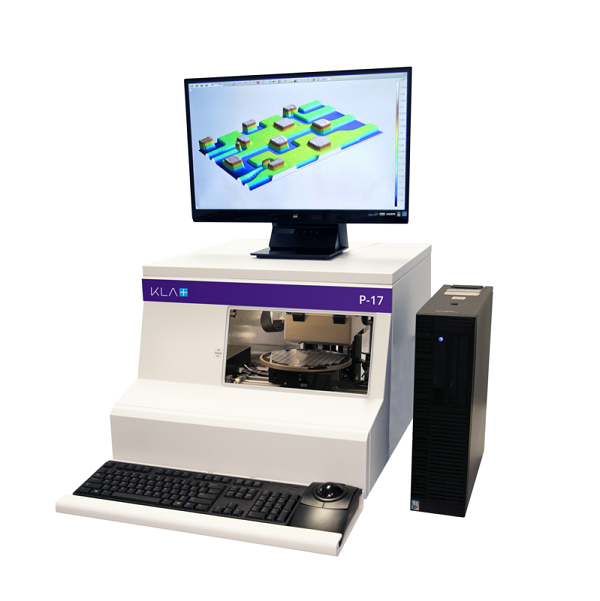
The P-17 is
an eighth generation benchtop stylus profiler, built on over 40 years of
surface metrology experience. This industry leading system supports 2D and 3D
measurements of step height, roughness, bow, and stress for scans up to 200mm
without stitching.
Excellent measurement stability is achieved with the combination of an UltraLite®sensor, constant force control and an ultra-flat scanning stage. Recipe setup is fast and easy with point-and-click stage controls, top and side view optics and a high-resolution camera with optical zoom. The P-17 supports 2D or 3D measurements, with a variety of filtering, leveling and analysis algorithms to quantify the surface topography. Fully automated measurements are achieved with pattern recognition, sequencing and feature detection.

II.Functions and Features
Features
· Step height: Nanometers to 1000µm
· Low force with constant force control: 0.03 to 50mg
· Scan full diameter of the sample without stitching
· Video: 5MP high-resolution color camera
· Arc correction: Removes error due to arc motion of the stylus
· Software: Easy-to-use software interface
· Production capability: Fully automated with sequencing, pattern recognition and SECS/GEM

Applications
· Step height: 2D and 3D step height
· Texture: 2D and 3D roughness and waviness
· Form: 2D and 3D bow and shape
· Stress: 2D and 3D thin film stress
· Defect review: 2D and 3D defect surface topography

Industries
· Universities, research labs and institutes
· Semiconductor and compound semiconductor
· LED: Light emitting diodes
· Solar
· MEMS: Micro-electro-mechanical systems
· Data storage
· Automotive
· Medical devices
· And more: Contact us with your requirements

III.Applications Details
Step Height
The P-17 is capable of measuring 2D and 3D step heights from nanometers to 1000µm. This enables quantification of material deposited or removed during etch, sputter, SIMS, deposition, spin coating, CMP and other processes. The P-17 has constant force control that dynamically adjusts to apply the same force on the sample surface, regardless of step height. This results in good measurement stability and enables accurate measurement of soft materials, such as photoresist.

Texture:
Roughness and Waviness
The P-17 measures 2D and 3D texture, quantifying the sample's roughness and waviness. Software filters separate the measurement into roughness and waviness components and calculate parameters, such as the root mean square (RMS) roughness.

Form: Bow and Shape
The P-17 can measure the 2D shape or bow of a surface. This includes measurement of wafer bow that can result from mismatch between layers during device fabrication, such as deposition of multiple layers for the production of semiconductor or compound semiconductor devices. The P-17 can also quantify the height and radius of curvature of structures, such as a lens.

Stress:
2D and 3D Thin Film Stress
The P-17 is capable of measuring stress induced during the manufacture of devices with multiple process layers, such as semiconductor or compound semiconductor devices. The bow of the surface is accurately measured using a stress chuck to support the sample in a neutral position. The change in shape from a process, such as film deposition, is then used to calculate the stress by applying Stoney's equation. 2D stress is measured with a single scan across the sample diameter for samples up to 200mm without the need to stitch. 3D stress is measured using a combination of 2D scans, with the theta stage rotating between scans to measure the full sample surface.

Defect
Review
Defect Review is used to measure the topography of defects, such as the depth of a scratch. Defect inspection tools identify defects and write the location coordinates to a KLARF file. The Defect Review feature reads the KLARF file, aligns the sample, and allows the user to select defects for 2D or 3D measurement.


