Norcada is a MEMS and photonic product
company specialized in the development and manufacturing of MEMS devices and
mid-IR DFB lasers for a wide range of industrial and scientific
applications. Founded in 2002, Norcada has a state-of-the-art MEMS and
photonics fabrication facility in Edmonton, Alberta, home to a major
nanotechnology cluster in Canada.
Norcada develops and manufactures MEMS devices for a wide range of
scientific applications. These products are fabricated using our proprietary
membrane platform technology and are sold world wide to high-tech companies,
national labs and universities in more than 30 countries. Our products include
silicon nitride grids for Transmission Electron Microscopy (TEM), membrane
devices for X-Ray microscopy, holders and MEMS chips for in-situ microscopy,
micropores, nanopores, single crystal silicon foils for radiation
physics. Norcada offers a wide array of standard products as well as
custom devices designed to meet specific customer needs using our platform
technology.
Technical
characteristics
Norcada is a MEMS and
photonics product company, specializing in the development and manufacturing of
MEMS devices and mid infrared DFB lasers, customized standard and non-standard
nitride windows, electrode integration, heating chips, electrochemical cells,
liquid battery components, hydrophobic and hydrophilic coatings, fault and FIB
TEM devices, lasers, nanopore products, etc.
Transmission Electron Microscopy:
Norcada designs and
manufactures a wide range of MEMS devices for Transmission Electron Microscopy
(TEM) applications, including low stress Silicon Nitride TEM Grids,
and MEMS chips for in-situ TEM work. Please click product icon on left for additional product information.
X-Ray Microscopy:
Our product line for X-Ray
microscopy applications include standard low stress silicon nitride X-Ray Windows
and MEMS chips for X-Ray Tomography work. Pleas click product icons on left for additional product
information.
In-Situ Microscopy:
Norcada offers a range of
MEMS products such as E-Chem chips, heating chips, liquid cells and X-ray
holders for in-situ electron and X-ray microscopy work. Please click here for
detailed product information.
Crystalline Silicon Membranes:
Norcada produces both
single-crystalline and poly-crystalline Silicon Membranes.
Single crystal silicon membranes are available in (100), (110), and (111)
crystal orientations. Please click here or
product icon on left for additional product information.
High Q-Factor Si3N4
Membranes:
These High-Q Si3N4 membranes are produced with stoichiometric silicon nitride films which have
extremely low mechanical dissipation (high mechanical Q-factor) and low optical
absorption, and are ideally suited for opto-mechanical studies. Click here or
product icon on left for detailed product information.
X-Ray Transmission Windows:
High performance and low
cost, Norcada’s X-ray transmission windows are ideally suited for X-ray
detector packaging and vacuum isolation applications. Please click here or producticon on left for product information.
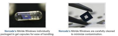
Custom Fabrication:
Norcada also provides custom fabrication of silicon nitride membrane
windows to meet our customer’s specific requirements. Such fabrication services
include non-standard sizes, thinner membranes, multi-window arrays, and windows
with patterned electrodes.
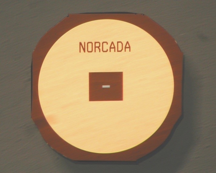
Standard silicon nitride
window
Standard silicon nitride
window grids for Transmission Electron Microscopy (TEM) are available with
5nm, 10nm, 30nm, 50nm, or 100nm thick square membrane windows centered on 200μm
thickness silicon frames. The TEM window frames are circular or octagon shaped
and fit inside a 3.0mm diameter circle. The silicon nitride membrane is low
stress and robust.
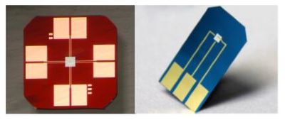
Liquid cell chip
The silicon nitride film
based MEMS chip designed and manufactured by Norcada can be used as a static
and dynamic liquid battery for in-situ electron microscope and X-ray
microscope.
It can be customized to fit
the customer's TEM. The chip can be designed as rectangle, square or polygon in
any size. The design of standard X-ray liquid chip fits Norcada holder and is
suitable for X-ray microscope application.
The silicon nitride window
on the chip can be customized in the thickness range of 10nm to 1000nm, and its
shape can be rectangular, square or circular.
The thickness of the spacer
can vary from nanometer to micrometer. Both open and closed designs are
available.
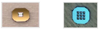
In-Situ heating chips
The heating chip can be
used for in-situ heating observation of large samples, with the maximum
measurable sample size of 1mm and the maximum temperature of 1100 ℃
Through software and
controller settings, each chip can realize temperature display and feedback
control.
The heating chip contains
at least 21 different heating element configurations, which can realize the
test of large and small samples, including the samples prepared by FIB, etc.
The heating device can work for several hours. In the range of 1000 ℃, the heating time is less
than or equal to 1 second, and the temperature measurement range is 0-1200 ℃. There is no external
water cooling system, and the cooling time is less than or equal to 1 second.

In-Situ biasing chips
Norcada offers a wide range
of MEMS e-biasing and e-chem chips for TEM, SEM applications. Norcada can also
offer customer tailored packages that include holders and MEMS
chips for STXM based applications. Norcada also designs and fabricate
MEMS chips with metal electrodes for electrical biasing and electro-chemical
study of samples during TEM analysis.
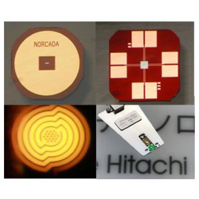
Norcada synchrotron
radiation holder
Suitable for soft and hard
X-ray applications
With Hitachi in situ TEM
and SEM
All compatible chip
adaptations
Configurable ventilation
In-situ heating and In-situ
biasing holder
The same sample holder can
provide in-situ heating and in-situ biasing testing functions. Easily switch
application mode by using different chips. The whole system can be easily and
simply installed in the vacuum chamber of electron microscope. The design of
in-situ chip is advanced and superior, which not only meets the conventional
application, but also can customize special in-situ chips according to the
characteristics of research. The same sample rack can provide in-situ heating
and in-situ bias test functions, and can also be compatible with FIB biasing
chip.