Introduction
Nanoimprint technology breaks through the difficulty of traditional lithography in the process of feature size reduction, and has the characteristics of high resolution, low cost and high yield.Since it was put forward in 1995, nanoimprint has undergone 14 years of development and evolved a variety of imprint technologies, which are widely used in semiconductor manufacturing, mems, biochips, biomedicine and other fields and are reputed as one of the ten technologies that have changed human beings.
The basic idea of NIL imprinter is to transfer the pattern to the corresponding substrate through the template. The transfer medium is usually a very thin polymer film, and its structure is hardened by hot pressing or irradiation to retain the transferred pattern. The whole process includes two processes: imprinting and pattern transfer. According to different imprint methods, NIL can be divided into three lithography technologies: Hot embossing, UV curing and Micro contact printing (uCP).
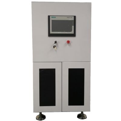
Main function
The main function of nanoimprint machine is to transfer the pattern to the corresponding substrate. The transfer medium is usually a very thin polymer film, and its structure is hardened by hot pressing or irradiation to retain the transferred pattern. Imprint technology is mainly divided into the following two types:
Hot pressing: firstly, a thin layer of thermoplastic polymer material (such as PMMA) is coated on the substrate, and the temperature is raised to reach the glass transition temperature (TG) of the thermoplastic material. When thermoplastic material is in a highly elastic state, a mold with nanometer scale is pressed on the mold and appropriate pressure is applied, and the thermoplastic material will fill the cavity in the mold. After the molding process is finished, the temperature is lowered to solidify the thermoplastic material, thereby obtaining a pattern coincident with the mold. The mold is then removed and anisotropic etching is performed to remove the remaining polymer. Next, the graphics are transferred. The pattern transfer can be performed by etching or stripping. Etching technology uses thermoplastic material as a mask to carry out anisotropic etching on the substrate below it to obtain corresponding patterns. In the stripping process, a layer of metal is plated on the surface first, then the polymer is dissolved by an organic solvent, and then the metal on the thermoplastic material is stripped, so that the metal is used as a mask on the substrate, and then etching is carried out to obtain a pattern.
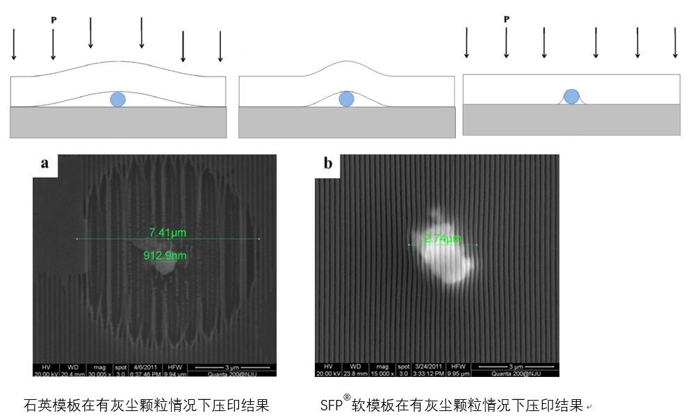
UV imprint: In order to improve the defects of thermal deformation in thermal imprint, C. G. willson and S. v. Sreenivasan of Texas University developed Step- Flash Imprint Lithography. In this process, ultraviolet transparent Quartz glass (hard mold) or PDMS (soft mold) is used, and photoresist glue adopts low viscosity, photocurable monomer solution. First, a monomer solution with low viscosity is dropped on the substrate to be imprinted. Combined with microelectronic technology, the film can be deposited by a spin coating method. The template is pressed onto the wafer with very low pressure to disperse the liquid and fill the cavity in the template. Ultraviolet exposure through the mold promotes polymerization and curing of the polymer in the imprinting region. Finally, the residual layer is etched and the pattern is transferred to obtain the structure with high aspect ratio. The final demolding and pattern transfer process is similar to the hot pressing process.
Update the research and development guidance of stamping process and document support
Technical competence
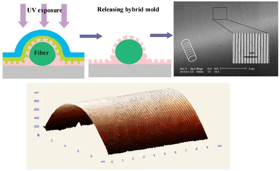
From 2001 to 2003, the inventor of the device worked as a research assistant for 3 years in the nanostructure laboratory of professor Stephen Y. Chou of Princeton university, the inventor of nanoimprint technology. he developed UV curing nanoimprint technology and materials and made important contributions to the development of nanoimprint technology. After joining the Department of Materials Science and Engineering in 2004, it continued its research work around nano-micro processing technology and nano-imprint technology, developed several new nano-imprint materials, developed new polymer imprint templates, and proposed curved nano-imprint technology. With the support of 863 project "research and application of UV curing and hot pressing dual-purpose nano-imprint equipment", the dual-purpose nano-imprint equipment with UV curing and hot pressing functions has been successfully developed and has become a product. it has been adopted by many universities and scientific research institutions such as Nanjing university, Beijing university of aeronautics and astronautics, national defense university of science and technology, Heilongjiang university, Shenzhen research institute of Chinese academy of sciences, etc. and has formed the core technology of nano-imprint with independent intellectual property rights. it has applied for and obtained a number of Chinese patents and U.S. patents, and its technical level is in line with the most advanced international level in this field.


